Gold Nanowire Ink Grids Used to Print Transparent Electronic Devices
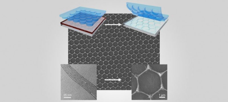
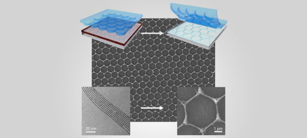
Today’s touchscreens, solar cells and thin film displays often contain transparent electronics devices. To produce these, transparent printable materials that remain highly conductive even when deformed are needed. To create flexible conductive grids with a resolution below one micrometer, the imprint process has been combined with a new self-assembling nano ink. The research was done at INM — Leibniz Institute for New Materials.
An ink of gold nanowires is applied to a substrate to print the grids. When a structured stamp is pressed onto the substrate, it forces the ink into a pattern. The nanowires adapt to any pattern of the stamp because they are so thin and flexible. The individual wires then self-assemble and form percolating bundles that are larger, resulting in a new grid being formed during the drying process. The grid is treated in a plasma after the stamp has been removed.
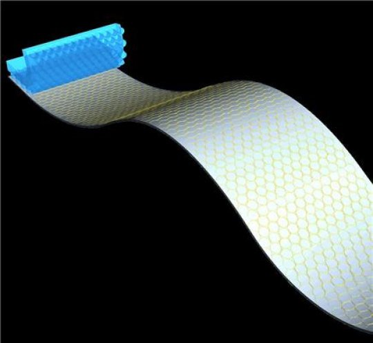
Tobias Kraus, head of the program division Structure Formation at INM, explained that the bundles are compressed into conductive wires by this process and this then forms a transparent, conductive grid. Any nano or microgrid can be shaped by using this simple method, with the geometry of the stamp determining the end shape.
The gold concentration is varied to control the thickness of the grid. This method uses far less gold than when using inks with spherical gold particles. As very small quantities of gold are needed as a result, the advantages of gold become accessible for the manufacturing of flexible electronics.
Transparent conductive materials can be efficiently produced using the self-assembly and imprint method and Kraus hopes to apply this insight to other metals in further studies.
Study has been published in the Nano Letters journal.
Save


