Deep dive: Hynix’s High Bandwidth Memory

We’ve discussed the capabilities and performance of HBM (High Bandwidth Memory) multiple timesover the past six months, but a new report sheds light on the physical architecture and construction of HBM. This new memory technology is viewed as the future of GPU memory. Nvidia will debut its own Pascal architecture in 2016 with HBM2, while AMD launched its own HBM-equipped GPUs, the Radeon Fury X and Radeon Fury, earlier this summer.
The full report by Tech Insights is paywalled, but the company shared a number of slides and details with EETimes. The HBM assembly that AMD and Hynix jointly designed is genuinely new compared to other products on the market. Samsung has used TSVs (through silicon vias) for wiring DRAM together before, but no one has ever built a wide I/O design like this in a commercial product.
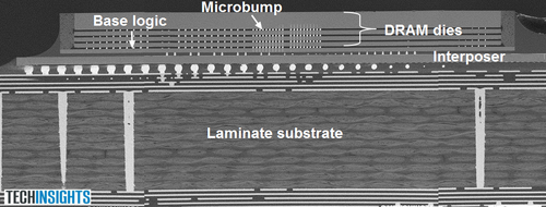
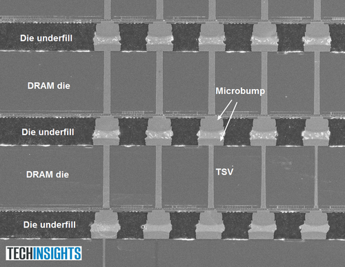
The image above shows the substrate, the interposer layer (manufactured by UMC on a 65nm process) and the stacked DRAM. The TSVs aren’t visible in this shot, but can be seen in the image below. The report also details how Hynix manufactured the TSVs and the process it used for creating them. One thing the authors note is that while they expected to see “scallops” in the images (scallops are ridges formed in the sidewall during the etching process), Hynix apparently did an excellent job avoiding the problem. Hynix, the author concludes, “has got a great etch recipe.”
The arrangement of the dies on the stack suggests that the first three DRAM dies were diced (cut from the wafer) as a group, while the top DRAM chip was cut separately, tested, and then attached to the stack. The entire four-die stack would then have been attached to the logic die. The advantage of this kind of configuration is that it offers Hynix ample opportunity to confirm that it’s building good die before attaching them in the final product.
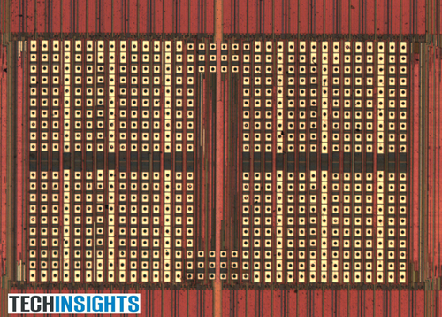
One piece of evidence in favor of this extensive test cycle is the sheer number of TSVs built into each DRAM. Tech Insights reports that there are nearly 2100 TSV pads on each DRAM die (one cross-section sample is shown below). In additional to being used for data, I/O, power, and redundancy, a significant percentage are apparently used to test the TSVs themselves. This fine-grained error control allows Hynix to determine exactly which TSVs aren’t meeting expectations and substitute one of the redundant TSVs where needed.
Why the fine details matter
Ever since AMD announced it would launch HBM, there have been rumors that HBM was either exceedingly expensive, yielding badly, or both. The Tech Insights excerpt doesn’t directly address either of these claims, but it does offer up some indirect evidence. Hynix has built a testing system that allows them to test for bad die at every level. They can test the stack of three ICs, they can test the top-level DRAM before mounting it, and they can test the TSVs after mounting and have a method of switching to redundant TSVs in case a bad link is found rather than tossing out the entire die stack.
The value of being able to test the product at multiple stages can’t be understated. Some of you may remember Rambus and its ill-fated attempt to conquer the DRAM market in the late 1990s and early 2000s. Rambus DIMMs were extremely expensive when they launched, and there were some conspiratorial whispers alleging that either Intel and Rambus were falsely inflating the price, or that the DRAM manufacturers were deliberately trying to cripple the product.
While the entire RDRAM situation was heavily political, one contact we spoke to at a memory company that was fully on-board with the RDRAM shift told us that no, there were real problems that crippled RDRAM yields. One of the most fundamental was that there was no way to test whether an individual RDRAM chip was good or not before mounting it in a series to make a RIMM module. If the module didn’t test perfectly, it had to be disassembled and swapped out, piece by piece, until a faulty IC was found. Since it was possible to have more than one faulty IC at a time, this step had to be performed using a “known good” set of chips until each RIMM was “known good.” Combined with the low yields that are typical for any ramping memory, this inability to test individual components contributed substantially to RDRAM’s high prices when it first launched.
By all accounts, Hynix hasn’t just rolled out a new solution by the skin of their teeth — they’ve built a scalable design that bodes well for the future of the memory standard. The interposer is built on a dirt-cheap 65nm process, and we already know HBM2 is ramping.


